
General information
Universidad Politécnica de Madrid
-
Research GroupLaser Center
-
Hosting Organisiation
-
AddressCampus Sur de la UPM. (Carretera de Valencia, km 7) Av. del Campus Sur 28031 Madrid
-
Contact Info:
-
Phone
-
Emaildirector.centrolaser@upm.es
Description
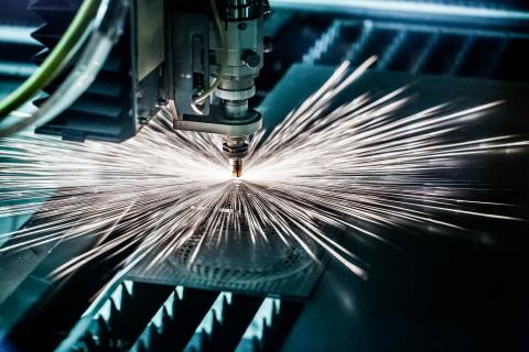
The main activity of the UPM Laser Center is applied to research in industrial processes based on laser technology for transfer to industry. Currently, the UPM Laser Center is a member of the Laboratories Hub of the FP7 APPOLO project, serving as a link between the European optoelectronic industry and different strategic industrial sectors to increase their productive capacity through the use of latest generation laser technology. The Laser Center is a research center that integrates two research groups: the Advanced Laser Manufacturing Group and the Research Group on Laser Engineering and Applications (GRIAL).
Summary of Research Services
His lines of research cover processes ranging from improving the mechanical properties of metallic materials through very high-power laser treatments, to tissue engineering in biomedicine through manufacturing based on transfer of biological material with lasers. The UPM Laser Center has a laser microfabrication service available to its users equipped with the latest generation systems and characterization laboratories with different microscopy techniques and material properties analysis.
Technology Capabilities
3D micromachining
Energy – Laser metallization of photovoltaic devices
Laser Texturing
Energy – a-Si Monolithic Interconnection
Energy - Laser cutting of battery electrodes
Energy - Laser Fired Contacts / Laser Doping
Bioengineering - Bioprinting
Numerical Simulation
High Speed Imaging
Research Group on Laser Engineering and Applications (GRIAL):
High Intensity Laser Materials Processing for Aerospace Applications (ESA, AIRBUS, ZAL).
Surface Micro-/Nano-Structuring for Energy Eciency and Carbon Capture.
Development of Advanced Alloys and Surface Treatments for Healthcare.
Numerical Simulation of High Intensity Laser Plasma Interaction (Mechanical and Advanced Energy Applications).
Development of Advanced Material Behaviour Models for Extreme Conditions.
Development of Models for Experience-Based Data Analysis and Process Control in Additive Manufacturing.
Main equipment or Facilities
Robotized Laser Processing Cell (6 DoF) including:
3,3 CW fiber transmited Nd:YAG Laser.
3,5 CW CO2 (slab) optically transmitted.
Hybrid Laser-Arc welding + heat treatment / cladding equipment.
Laser Shock Processing Cell including:
Pulsed (2,5 J, 10 ns, 10 Hz) Nd:YAG Laser.
6 DoF Robotized positioning system.
Spectroscopic + fast camera Plasma analysis system.
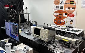
Laser microprocessing lab., including:
Microprocessing workstation OPTEC ML-100 equipped with KrF + Nd:YVO4 (mW range) ns lasers.
Microprocessing workstation OPTEC AB-200 equipped with PULSEO (100 kHz, 25 ns, 10W) and VANGUARD (80 MHz, 20 ps, 8 W) Nd:YVO4 lasers.
Mechanical testing laboratory equipped with MTS 100 kN system.
Microscopy (SEM + confocal) and Surface Characterization (wear, corrosión, residual stresses) laboratories.
For the development of models for the predictive assessment of laser processing applications, the Group operates a moderate range workstation based computational centre.
Software, tools or licenses to be applied to Big Science:
COMSOL software.
High Speed Imaging System (25 ns resolution).
Advanced Laser Based Manufacturing Group:
Micromachining Laser Stations
AB 200- UV nano-picoseconds:
Spectra Physics Pulseo (DPSS Nd:YVO4, 20 ns, 20W @ 100kHz).
Spectra Physics Vanguard (DPSS Nd:YVO4, 10 ps, 80 MHz, 350 mW).
ML 100- UV nanoseconds:
ATL Laser Lasertechnik SP300i (KrF excimer 248 nm, 7ns, 5 W@300 Hz).
Spectra Physics HIPPO (DPSS Nd:YVO4 355 nm , 15 ns, 5 W @ 50 kHz.
INNOLAS Lumera Superapid-picoseconds:
DPSS Nd:YVO4 1064 nm/ 532 nm/ 355 nm 8 ps.
18W @1064 nm / 8W @ 532 nm / 4W @ 355 nm.
Appolo Hub Workbench
Application Laboratory for Equipment Assessment in Laser Based Manufacturing.
Biological Lab Facility for Laser Bioprinting
Microscopy Facilities
Raman Microscopy Renishaw inVía.
Confocal Microscope Leica DCM 3D.
Scanning Electron Microscopy Hitachi 3000 N (SEM-EDX).