
General information
Universidad Politécnica de Madrid
-
Research GroupInstitute for Optoelectronic Systems and Microtechnology (ISOM)
-
Hosting Organisiation
-
AddressISOM-UPM ETSI Telecomunicación Avenida Complutense, 30. 28040 Madrid, España
-
Contact Info:
-
Phone
-
Emailsecretaria.isom@upm.es
Description
The Institute for Optoelectronic Systems and Microtechnology (ISOM) is a multi-departmental research institution devoted to graduate research and education in electrical engineering, which is affiliated to the Universidad Politécnica de Madrid (UPM). ISOM was created on March 16th 2000 as the result of the proposal presented by several research groups from the departments of Electrical Engineering, Photonic Technology, Applied Physics to Information Technology and Applied Physics to Architecture and Environment. This personnel is divided in two research groups: Semiconductor Devices Group (GDS) and Magnetic Devices Group (GDM). Its size as well as the large experience in research during the last two decades, in particular participating in numerous projects funded by the European Union, make this team distinctively well suited for research and development activities.
ISOM is a node in the ICTS (Unique Scientific and Technical Insfrastuctures) distributed Network of White Rooms for Micronanofabrication (MICRONANOFABS) of the Spanish Ministry of Science and Innovation. Currently, we have been included in the European Network of White Rooms called EURONANOLAB.
Summary of Research Services
Green enery and environment
Information and communications
Nanomaterials and emerging applications
Technology Capabilities
2D Materials
Nanophotonics and IR plasmonics
Spintronics
SAW-based devices
Epitaxy of nanostructures (LEDs, LDs,…)
Magnetic sensors and devices
Main equipment or Facilities
ISOM facilities include a 400 m2 cleanroom (100-1000 class), and 300 m2 of characterization and processing laboratories. In addition, there are areas dedicated both to Industrial Cooperation and Technology Transfer and External Services.
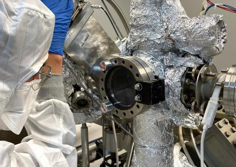
Inside the cleanroom among many processing apparatus such as e-beam evaporators, annealing ovens and there are several crystal growth systems including molecular beam epitaxy for nitrides, arsenides and antimonides, chemical vapor deposition for graphene and sputtering for piezoelectric and magnetic materials. A class 100 lab inside the cleanroom is dedicated for the optical lithography and one of the most powerful e-beam lithography systems available (10 nm per line).
The characterization labs include a scanning electron microscope equipped with cathodeluminescence (UV,VIS,IR) and EDX, a atomic force microscope, optical benches for cryostats for UV, VIS, IR photoluminescence, X-ray diffractometers and Probe stations for measuring at room, low and high temperatures.