General information
-
Hosting OrganisationCeit
-
AddressPaseo Manuel Lardizabal 15, 20018 Donostia-San Sebastián
-
Contact Info:
-
Phone
-
Emailinfoceit@ceit.es
Description
Ceit is a nonprofit private research center with the mission to serve the industrial sector, carrying out projects of applied research and technological development. Ceit is a multidisciplinary center, whose work is oriented to different sectors: railway, aeronautical, automotive, health, manufacturing, energy, environment and ICT.
Summary of Research Services
CEIT offers R&D projects tailored to industry needs, a pilot plant for atomization of special powders, and advanced material characterization (structural, chemical, thermal, and optical). Expertise includes artificial intelligence, robotics, digital twins, electrification, sustainable transport, and circular economy.
Technology Capabilities
Ceit's capabilities and interest with regard to large scientific facilities are:
- Development of materials and components for extreme environments: graphitic materials, self-passivating W alloys, ODS Steels, EUROFER, CuCrZr, porous silicon carbon with tailored porosity.
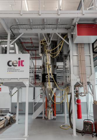
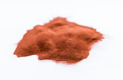
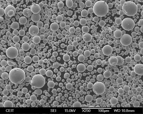
- Design, production and processing of powders. Equipment with metal/gas atomizer to produce tailored metallic powders for Additive Manufacturing or (Near) Net Shape technologies. From 1 kg up to 250 kg of powder with composition within ITER/EUROfusion specifications: ODS Steels, EUROFER, CuCrZr, Cu-OHF.
- HIP. Consolidation of ceramic and metallic powders encapsulated in cannisters, removal of residual porosity in castings or components obtained by Additive Manufacturing.
- Additive Manufacturing: PBF-LB (powder bed fusion laser beam), BJ (Binder Jetting), wire and powder DED-L (laser beam directed energy deposition).
- High precision Femtosecond Laser surface processing.
- Solid state diffusion bonding of Cu, CuCrZr, AISI 316L, EUROFER, ODS steels and tungsten.
- Failure analysis. Identification of failure mechanism (mechanical and thermomechanical fatigue, fractography analysis...). Advanced techniques for residual stresses measurement.
- Electronic and magnetic NDT for microstructural characterization and identification of defects and cracks.
- Thermal Physical, mechanical and microstructural characterization (SEM, TEM, AFM).
-Remote handling: haptic devices (mechatronics background), control engineering (teleoperation, mobile cobots, low latency communication systems like 5G), own XR technology for remote asistance, 2D and 3D vision for metrology, quality inspection
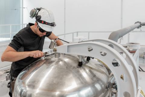
Main equipment or Facilities
*Spray Atomization Pilot Plant:
- Metal/gas atomizers for producing metallic powders
- Supports additive manufacturing and near-net-shape forming
*Thermomechanical Processing & Powder Metallurgy Labs
- Development of advanced alloys (tungsten, EUROFER, ceramics)
- Techniques: Hot Isostatic Pressing (HIP), femtosecond laser treatments
*Advanced Manufacturing Facilities
- Additive manufacturing: PBF-LB, Binder Jetting, DED-L
- Solid-state joining and precision component fabrication
*Mechanical Testing & Non-Destructive Evaluation Labs
- Material and structural behavior analysis
- Ensures reliability and integrity under operational conditions
*Electronics & Communication Labs
- Design and testing of electronic systems
- Applications: electric vehicles, smart grids, advanced communication systems